Radiation Effects in Silicon
Peter Voss
1. Introduction
Any silicon device that has left the manufacturing process and goes
into an application will be exposed to some degree of high-energy
electromagnetic or particle radiation. Most devices, however, have seen
the highest degree of exposure to particle irradiation already during
the manufacturing process, the most common irradiation process being
ion implantation. Less common is the exposure of silicon intended for
the manufacture of high-voltage power devices to high fluences of
low-energy neutrons for the purpose of neutron transmutation doping and
these bipolar devices may also have been exposed to the various methods
using high-energy electrons, protons, alpha particles and gamma rays to
adjust carrier lifetimes or doping levels. These methods will be
described in this section.
Most applications of silicon devices take place at ground level where
the devices are exposed to a low rate background radiation originating
from radioactive materials in the device or in the package or from
cosmic rays. A sizable number of devices is used in airplanes which
during flight are exposed to a level of cosmic ray radiation about 300
times that at ground level and some devices are operated in space
environments or close to particle accelerators where the radiation
level can be quite high and can lead to degradation or various upsets
of the devices. We will also look into these aspects of device
irradiation.
2. Interaction of radiation with silicon
Depending on whether the interaction of a silicon device with
radiation occurs already during the manufacturing stage or during its
application, different aspects of the interaction are of interest.
During the manufacturing process it is predominantly the incorporation
of ions as dopants or the generation of crystal defects that act either
as recombination centers or as dopants, while during application the
focus is on the charge generated by single particles - either by the
particle itself or as secondary charge after a nuclear reaction - , or
the focus is on the long term degradation and doping effects after
high-fluence exposures which then are often similar to those effects
employed during manufacturing in a prescribed way. Naturally, the ions
used in the manufacturing process and the particles encountered by a
device during application are seldom of the same kind. There is often
also a significant difference in the energies the particles or the
electromagnetic radiation posess. Ion implantation energies are
typically in the keV range. Energies for the intentional introduction
of damage are typically of the order of a few MeV, while the energies
of cosmic ray particles reach into the GeV range and way beyond.
When high-energy particles are used for processing silicon, the main
interest is in an exact determination of the dosage, in obtaining the
right penetration depth and in the annealing procedures for undesired
crystal defects. When particles can interact with the finished device
in an application, one has to find ways to determine the probability
for single event effects (SEE) due to the charge or the damage
generated during a specific operation mode. When the finished device is
exposed to continuous high fluxes of radiation, there is usually no
possibility to at least partially anneal the generated defects in
regular cycles, though there are applications where this is the only
way to guarantee long term operation.
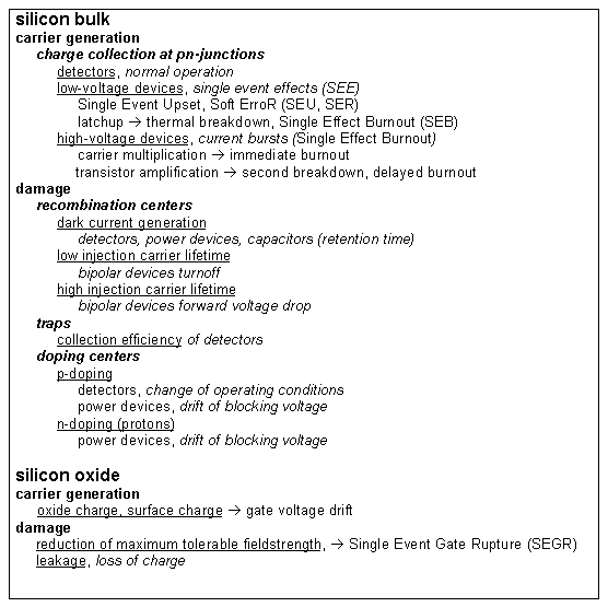
Tab. 1 lists a number of typical effects of the various types of radiation.
Tab. 1 Various effects of radiation in silicon and silicon oxide
The reasons for deteriorations and upsets of silicon devices fall into
a few basic categories, but the consequences are very widespread.
The most elementary effect is the generation of charge in the silicon
bulk by the absorbed particle. In a detector the charge gives rise to
the current pulse to be analyzed. In this case an undisturbed signal
with high collection efficiency is desired. Similar current pulses
occur in any circuit that has a charge collecting capability. Depending
on how the collecting cell is interconnected with neighboring cells the
current pulse can lead to upsets. The details depend on the current
shape, operating voltage etc.. In the capacitor cell of a memory device
it is the change in the charge of the cell itself that may flip its
logic state. In arrangements with simple pn-junctions or in surface
counter arrangements the local disturbance of the field distribution
can cause avalanche multiplication and possible destruction. In
multilayered structures there may be parasitic transistors incorporated
that react to a primary current pulse and cause latchup of a device or
device cell and in unfavorable situations may lead to destructive
second breakdown due to thermal runaway.
Finally there is the effect of the generated lattice defects that in
bipolar devices cause a change in carrier lifetime. Often the
concurrent increase in dark current through the radiation-induced
recombination centers is of equal or even more concern.
When the particle is absorbed in an insulating layer of silicon oxide
or silicon nitrite, most of this charge is trapped in the layer or at
its surface. It can be moved either through high electric fields or
dissipated through elevated temperatures. In MOS devices the changes
resulting from the trapped charge normally have detrimental effects,
e.g. when the gate voltage changes, but such change can also be taken
advantage of in dosimeters. When the movement of the generated charge
takes place immediately after generation, it may result in oxide
breakdown, i.e. in gate rupture.
2.1. Particles
2.1.1. Protons, alpha-particles, heavy ions
The status of the ways to determine the stopping of high-energy
particles in solids is reviewed in [1]. Ziegler and Biersack developed
a program, TRIM or SRIM [2], for calculating the stopping and range of
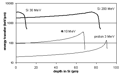
ions in solids. Some examples are given in Fig. 1. The energy transfer
or stopping power is given versus penetration depth. For clarity,
energy transfer is presented here in units of keV/µm, whereas it
is usually plotted as MeV/mg/cm2. The scaling factor is 1 keV/µm
= 4.31 keV/mg/cm2. All these examples are for energies in the MeV
range, i.e. significantly higher than used for ion implantation. The
curves for protons and alpha particles are examples for energies used
for lifetime adjustment or for energies of particles originating from
radioactivity or cosmic rays. The curve pertaining to silicon ion
energy of 30 MeV is an example for a high energy recoil of a
nuclear reaction which might result from a collision of a high-energy
neutron with a silicon nucleus. The 200 MeV curve is shown to
demonstrate the different shapes of the stopping power curves. Stopping
power is usually abbreviated as LET for 'Linear Energy Transfer', which
is obviously not a good description for the lighter particles.
Fig. 1 Stopping power of protons, alpha particles and silicon ions in silicon
calculated with TRIM [2]
The interaction of the ions causes displacement of the recoil
atoms of the target and gives rise to interstitial atoms and lattice
vacancies. Interstitials and vacancies have a high mobility even at
room temperature and become less mobile by forming complexes or by
attaching to dopants in the silicon, in the bulk first of all to carbon
or oxygen which are usually present at concentrations around 1015 cm3,
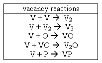
or in case of oxygen even higher. It appears that the vacancy reactions
are particularly important. Table 2 shows a number of possible
combinations.
Tab. 2 Radiation damage vacancy reactions, from [3]
Of these reaction products the divacancy and the vacancy-oxygen complex
are effective as recombination centers, whereas the divacancy-oxygen
complex forms an acceptor level. The effectiveness in one or the other
way depends on the position of the level in the band gap, on the
capture cross section for electrons and holes and on the position of
the Fermi-level. For details see for example Baliga [4]. Recombination
processes for the low and the high injection case can generally be
described on the basis of the Shockley-Read-Hall model [4] with one or
several single-level recombination centers. This approach apparently
has failed for the modeling of dark currents when the damage is
generated by high-energy particles, where it results in current levels
that are two orders of magnitude too low [5]. The observed high dark
current levels are assumed to be caused by the overlap of
recombination levels generated in damage clusters [6].
In the normal implantation process for doping purposes all damage is
annealed as much as possible, whereas when radiation is used for
trimming of device properties one obviously wants to retain at least
some of the generated defects or complexes. In these cases one main
aspect of the treatment after implantation is that the finished device
has to have stable electrical properties in the range of application.
For many high-voltage power devices the maximum application temperature
reaches only up to 125 °C or 140 °C. In such cases an annealing
process at a temperature of 250 °C over several hours has proved to
be sufficient. Most defects can be annealed at temperatures around 350
°C, but - depending on the preprocessing - defects can be stable
well beyond a temperature of 450 °C.
Implantation of protons or helium ions is predominantly used in order
to adjust carrier lifetime in bipolar devices. As can be seen from Fig.
1, using protons has the advantage that the energy transfer is highly
localized in the region where the proton comes to rest and
therefore almost all the damage is generated there. As can be seen in
Fig. 1 to a lesser degree this also holds true for helium ions. In this
way one can insert regions of increased local carrier recombination
rate. For some applications proton implantation has the disadvantage
that when a high dosage is required the implanted hydrogen causes a
n-doping that may affect the breakdown voltage of the treated device in
an undesired fashion [7]. Naturally, this behavior can also be used as
an additional process tool in some instances. Helium ions and any
heavier ions cause p-doping via the V2O-center, but in case of helium
at a much lower generation rate as compared to protons.
2.1.2. Electrons
In comparison to heavier particles, electrons have a much higher
penetration depth and are therefore well suited when uniform generation
of damage is required. Electron irradiation has become a standard
method for the adjustment of the carrier lifetime in large area power
devices like diodes and thyristors. These device often have very
stringent requirement with regard to their blocking behavior, which in
case of thyristors is governed by dark current generation in the
space charge region and the low injection carrier lifetime outside of
it. The dynamic behavior of these devices during turn-off as a
trade-off with respect to the forward conducting behavior is governed
by the carrier lifetimes for high and low injection.
Electron irradiation has to a large extent replaced conventional
diffusion methods of lifetime control like doping with gold or
platinum. This is largely due to the convenience of being able to do an
exact lifetime trimming, but for high-voltage devices also to a large
extent because of the requirement for the blocking current to be as low
as possible. For some medium-voltage devices for which the dynamic
properties are often most critical, it is still not unusual to combine
conventional diffusion techniques and radiation techniques to achieve
optimum properties for the carrier lifetime.
Work on electron irradiation started with electrons having energies
below 2 MeV and did not look very promising when the results were
compared with gold diffusion. Similar unpromising results were obtained
with gamma rays (the highest transfer energy to electrons is 1.1 MeV).
It was only after it was shown that higher electron energies yield a
better trade-off that electron irradiation became widely used. Fig. 2
shows the results of the first investigation of the influence of the
electron energy [8].
Originally it was thought that the divacancy was the main generated
recombination center, but currently there are indications that the VO
center (A-center) is dominant. This is supported by the fact that
lifetime measurements on electron irradiated unprocessed float-zone
silicon wafers (oxygen content < 1*1015 cm3) have indicated
drastically reduced generation rates for the recombination centers.
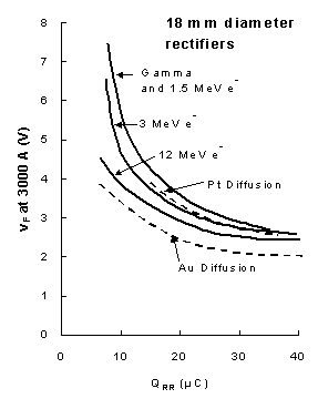
Fig. 2 Forward voltage drop
versus reverse recovery current for diodes irradiated with gamma rays
or electrons as compared to diodes diffused with platinum or gold [8]
2.1.3. Neutrons
Neutrons are considered here because they are the main contributors to
single event effects at ground level. They are generated in particle
showers that occur when high-energy particles hit the outer atmosphere
of the earth. Due to their electrical neutrality neutrons will not
interact with the electron gas as protons do and therefore they have a
larger penetration depth in matter than the latter. Interaction takes
place solely with the atomic nuclei. At energies above approximately
100 MeV the stopping mechanism for neutrons and protons becomes
similar. This is an important feature when it comes to testing devices
for cosmic ray failure rates.
2.2. Nuclear reactions
When solids are irradiated with particles, nuclear reactions with the
target set in at approximately 1 MeV/amu particle energy, where amu
stands for atomic mass unit. During device processing this is a side
effect that may deserve some attention because of the resulting
radioactivity. On the other hand, nuclear reactions are the major cause
for single event effects at ground level and in the atmosphere. Single
event upsets in signal processing devices are first of all due to the
charge generated per unit volume. Experimental experience shows that
the charge generated by a proton is usually not sufficient to cause an
upset, whereas the denser charge tracks of helium ions (compare Fig. 1)
originating from packaging material polluted with minute traces of
alpha emitters were historically the first obvious causes for upsets at
ground level. Any particle heavier than helium can cause upsets.
Heavier nuclei are generated when a primary particle, e.g. a
high-energy neutron or proton, collides with a silicon atom. This
results in a large variety of fission products, light fractions like
alpha particles and heavier fractions, in the case of silicon
predominantly ranging from carbon to silicon.
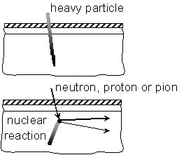
Fig. 3 Schematical representation of heavy ion or lighter particles
being absorbed in a metallized junction device
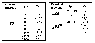
Tab. 3 Examples of spallation events with 150 MeV protons incident on silicon [10]
Tab. 3 shows selected results from calculations of Tang using the
simulator NUSPA[9] of spallation products from nuclear events after
collisions of 150 MeV protons with silicon [10], indicating the
diversity of the secondary products and of their energies. Recoiling Si
atoms constitute the largest fraction at low energies, whereas there is
a considerable amount of high-energy oxygen and carbon atoms with
energies reaching up to about 30 MeV.
In integrated memory and logic devices the unit cells are small and
therefore not all the generated charge may be deposited in the cell
where the reaction occurs. Depending on the flight path of the
secondary particles several cells may be affected, leading to multiple
upsets. For these devices the generated charge is of main concern.
However, in charge storing junctions the damage may lead to an increase
in dark current to such a degree that the retention time is strongly
reduced and that in extreme cases the stored information is lost.
Depending on the design of the cell, a relatively large amount of
charge may be collected due to diffusion or due to a distortion of the
space charge region by the ion track, leading to charge funneling [11].
The distortion of the space charge region by the ion track can cause
drastic results in high-voltage power devices when it initiates
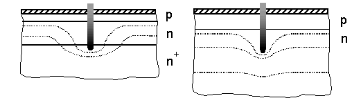
avalanche carrier multiplication. Schematical representations of space
charge region distortions are depicted in Fig. 4.
Fig. 4 Schematical representation
of the effect of ion tracks in a low-voltage and in a high-voltage
device. Dashed lines indicate equal potential lines.
In the low-voltage device the space charge region expands into the
highly doped substrate and may no longer be able to support the
original voltage.
Charge generated in the substrate will be collected at the junction
(funneling). In the high-voltage device the space charge region also
expands.
The fieldstrength at the tip of the ion track may become so high that carrier multiplication sets in.
3. Radiation sources
3.1. Natural radiation background
The first single event effects in silicon devices that could be traced
to their origin were caused by alpha particles emanated by the
packaging material or by the metallization [12,13 ]. These causes have
been reduced to a large extend, but are by no means completely
eliminated. The main natural radiation background affecting silicon
devices originates from cosmic rays.
In outer space protons are most abundant, largely as part of the solar
wind with energies into the MeV range, whereas protons from deeper
space can have energies as high 1020 eV. Cosmic rays also contain
heavier ions, mainly iron.
The earth atmosphere shields most of this radiation. High-energy
particles penetrating the earth's outer atmosphere lose their energy
through nuclear reactions with the air molecules and cause showers of
secondary particles. The atmosphere of the earth provides a shielding
of about
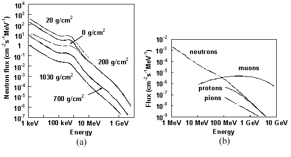
Fig. 5a Neutron flux vs.
altitude. 1030 g/cm2 corresponds to sea level, 200 g/cm2 to a height of
10 km, i.e. to airplane cruising level. Detail from [14].
Fig.5b Theoretical curves of flux of cosmic rays at New York City. From [14].
1 kg/cm2. For the secondary particles to reach ground level, the energy
of a primary proton has to be of the order of 1 GeV. Since the energy
of the primary particle can be much higher, the energies of the
secondary particles in the shower can reach beyond 1 GeV (Fig. 5b). Due
to the influence of the solar wind on the earth's magnetic shielding,
cosmic radiation at ground level is actually reduced in times of
increased solar activity.
The highest density of particles is reached at a height of about 18 km
above ground (Pfotzer peak). Fig. 5a shows a plot of the neutron flux
versus energy for different heights [14]. The way this diagram is
plotted on a logarithmic scale, a one decade decrease of neutron flux
of per decade of energy means equal numbers of incident particles per
decade energy. Fig. 5b depicts the flux at ground level [14]. At high
energies muons dominate, but since these have a very low absorption
coefficient they play a very minor role with respect to upsets as
compared to the other particles. At ground level neutrons cause most
interactions.
3.2. Exposure to radiation during operation
The natural radiation background is of concern for a number of failure
modes. Some of these failures may just be a nuisance to the end user,
others lead to total failure of a piece of equipment and some may even
endanger human life when they occur in the electronics of
defibrillators or of pacemakers.
Deterioration of device properties, upsets and failures were naturally
first encountered with devices operated in highly ionizing
environments, e.g. when they were used as radiation detectors or in
space applications. The airplane industry was next to realize this
problem and only fairly recently has it become obvious that cosmic rays
can be a rather serious problem at ground level, in particular for
power devices.
Silicon devices are increasingly used as radiation detectors in
accelerator facilities under conditions where they are exposed to
extreme rates of radiation.
Electronics operated in space are exposed to high levels of radiation
in the radiation belts of the earth or other planets and during
bursts of the solar wind. The spacecraft community has learned to live
with this problem, since it is unavoidable. Spacecraft can be shielded
to some degree against heavy particles and partly also against the
lower energy lighter particles consisting mostly of protons. Special
device designs enable radiation-hardened features. Error detection and
correction codes (EDADCs) eliminate most if not all bit losses in
digital equipment. But as more electronic parts are used in spacecraft,
e.g. as hydraulically operated parts are replaced by power electronics,
new failure modes surface. Some of these are modes of total failure, so
that the question of tolerable levels for total failure is becoming
more important. A general tendency for all devices seems to be an
attempt to use commercial (COTS - Commercial Off The Shelf) parts as
much as possible instead of special hardened designs, because the
performance of the latter is often several generations behind that of
state-of-the-art parts.
3.3. Prediction of SEEs
For any kind of application in a radiation environment it is essential
to have an understanding of the upset and failure rates to be expected.
The prediction of SEE events can be relatively simple for devices like
diodes operated at ground level, where, e.g. a test with neutrons or
protons at one energy gives results that can be directly matched with
reference results. On the other hand, predictions can become very
complicated when complex electronics parts, the details of which are
often unknown to the user, are used in space under constantly changing
radiation conditions.
Several codes have been developed for SEE prediction by manufacturers
and users. These incorporate either all the details of the nuclear
events and of the circuitry of the device for performing Monte Carlo
calculations or they are based on accelerator testing of basic
structures or complete devices under various conditions with respect to
particles, particle energies, irradiation angles and device operation
conditions. Details are given in [15], [16], [10] and [17].
3.4. Accelerators
For the various methods of irradiation treatment and for accelerated
tests of various failure modes a variety of accelerators is required.
High-energy electron accelerators used to be relatively rare, but
lately there has been a proliferation of new industrial facilities with
the capability to scan large areas. These installations have typical
energies of the order of 10 MeV.
The requirements for other particle accelerators depend on whether they
are needed for processing or for testing. Processing as treated here
does not include standard ion implantation methods, i.e. it refers
mainly to proton and helium implantation. A proton implantation of 50
µm requires an energy of about 2 MeV (see Fig.1). Such energies
can be achieved with tandem van-de-Graaf or dynamitron machines.
For tests that try to reproduce cosmic ray conditions larger facilities
are needed. A number of accelerators are available for routine testing
with protons, neutrons and heavy ions. Proton energies reach up to 1
GeV. A survey is given in [18]. Testing in these installations is
rather costly and therefore one tries to keep these test at a minimum.
4. Device exposure to ionizing radiation
4.1. Adjusting device parameters
Radiation as a means to adjust device parameters is mainly used with
high-power bipolar devices. As already shown in the example of Fig. 2,
one wants to achieve the optimum trade-off for these devices between
forward voltage and dynamic properties like reverse recovery charge or
turn-off time or one intends to optimize for a specific turn-off
behavior with respect to the way the current flow ceases during
turn-off. Electron irradiation with energies above 4 MeV in many cases
has proved to provide a good compromise with respect to low dark
current levels and low carrier lifetimes under low and high injection
conditions [4]. This applies first of all to thyristors that have
symmetric blocking characteristics in forward and reverse direction
where any unsymmetric type of irradiation usually causes a strong
deterioration in one direction. Assuming that the generation of
recombination centers is proportional to the dosage, it is generally
assumed [19] that the change in carrier lifetime follows the law
1/tau = 1/tau0 + const * dosage
where tau0 is the carrier lifetime before
irradiation. The damage constant is strongly dependent on the
processing history of the device, in particular on the level of oxygen
doping. Usually carrier lifetime cannot easily be determined directly
and therefore similar relations are used for the reverse recovery
charge (Qr) or the turn-off time (tq). Since the relation between these
properties and carrier lifetime depends on measurement conditions and
device design, such assumptions usually hold only over a narrow range.
Usually 1/Qr and 1/tq increase more than proportionally with dosage.
For asymmetric devices like diodes, proton or helium irradiation offers
an additional degree of freedom, since the carrier lifetime can be
reduced locally (see Fig. 1). This has proved to be very useful for the
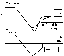
adjustment of the turn-off behavior of diodes for which a 'soft'
turn-off behavior is often desired, as a contrast to a 'hard' turn-off
or 'snap-off' behavior that may lead to a destruction of the device or
to undesirable circuit ringing (Fig.6). With the local lifetime control
one can generate pockets with higher carrier lifetime serving as
carrier reservoirs which supply the carriers for the soft current tail
part [20].
Fig. 6 Schematics of various diode current transients during turn-off
In these applications the n-doping effect of implanted protons is
sometimes detrimental, and therefore helium is preferred for which a
p-doping occurs only at much higher doses. However, in cases where the
local breakdown voltage of a device is to be adjusted, the n-doping as
well as the p-doping effects of protons and of helium ion damage,
respectively, can be used [21]. These methods have to be used with
care, though, when there is the possibility of self-annealing due to
strong local heating during operation.
4.2. Examples for radiation effects in applications
A few typical examples will be given here for the various effects
caused by ionizing radiation. Many of these examples are taken from the
records of the 'Annual International Nuclear and Space Radiation
Effects (NSREC)' Conferences and the 'Radiation and its Effects on
Components and Systems (RADECS)' Conferences [22]. A review on
terrestrial cosmic rays and SEUs caused by these is given in [23].
4.2.1. Detectors in high-dosage environment
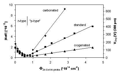
The SMS Tracker experiment at CERN will contain 200 m2 of silicon
detectors [24]. These detectors are expected to survive a total flux
of 3*1015 high-energy particles per cm2 over a period of 10
years. It was shown that this task can probably be achieved, though
with rather unusual consequences for the devices. For tests the
detectors were produced from very low n-doped wafers 300 µm thick
with n- and p-diffusions on either side, respectively. The final
devices will be operated at 600 V. The main concern during the
operation of these devices will be the change in doping level due to
the formation of divacancy-oxygen centers and the concurrent increase
in dark current.
Fig. 7 depicts results showing the change of effective doping depending
on the dose of 24 GeV protons and on the carbon and oxygen content of
the bulk material. The 'carbonated' silicon had a carbon content of
approximately 2*1016 cm-3 whereas the 'oxygenated' silicon had an
oxygen content of approximately 3*1017 cm-3 At a dose of approximately
0,7*1014 protons/cm2 the effective doping of the bulk material changes
from n-type to p-type. Fig. 7 also shows the voltage VDep necessary to
have the entire 300 µm wide bulk region depleted. High oxygen
content shifts the equilibrium from V2O + O to 2VO, i.e. from doping to
recombination centers, and in this way makes the devices less
sensitive. When the bulk resistivity goes from n-type to p-type the
junction moves from one side of the wafer to the other. Since
these detectors are intended for high-energy particle measurements,
this shift apparently does not affect the operation.
Fig. 7 Dependence of acceptor generation on proton dosage and bulk doping. VDep is the voltage necessary to expand the space charge region across the 300 µm width of the bulk region [24].
In contrast to the results in Fig. 7, the dark current does not show
any dependence on bulk impurities. It depends only on the energy of the
particles used and on whether particle energy generates only point
defects or suffices to generate defects in clusters. In the latter case
there is a linear dependence on dosage [5]. Gamma rays and low energy
electrons generate only point defects leading to a dark current lower
by two orders of magnitude. In the transition region there is seemingly
a quadratic dependence on dosage [5].
4.2.2. Memory cells (DRAMs and SRAMs)
In DRAMs the information is stored as charge in a capacitor cell. Since
the capacitor discharges with time the charge has to be replenished in
regular cycles. Critical for these cells therefore is the amount of
stored charge and the retention time. An ionizing event can upset the
charge state of the cell and the damage occurring alongside can reduce
the retention time, possibly to the point where it falls below the
replenishing time (stuck bit [25]).
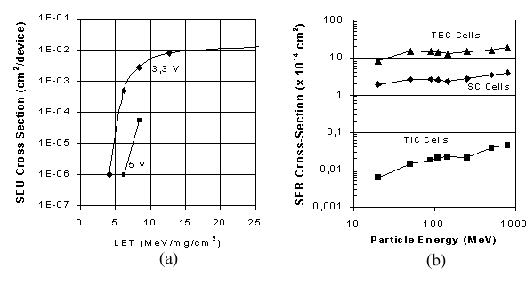
The sensitivity of a cell is defined in terms of a critical charge or
in terms of a cross section in dependence on the energy transfer (LET)
of various particles or on energy of one type particle. Fig. 8a and
Fig. 8b are examples plots of such dependencies. Fig 8a depicts a
typical behavior [26]. The upset cross section rises steeply beyond a
minimum energy transfer and saturates at high LETs. The threshold of
the LET depends on the operating voltage, but, e.g., also on the angle
of incidence. In this particular device the threshold is so high that
this device is insensitive to alpha particles (compare Fig. 1).
As the size of DRAM cells is steadily decreased with every new
generation, there is a general tendency for the cells to become more
sensitive to upsets. However, device designers have become aware of the
problem and changes in the layout of the cells have compensated this
trend. Fig. 8b shows for three different types of 16 MB-DRAMs a plot of
the upset cross section versus proton energy [27].
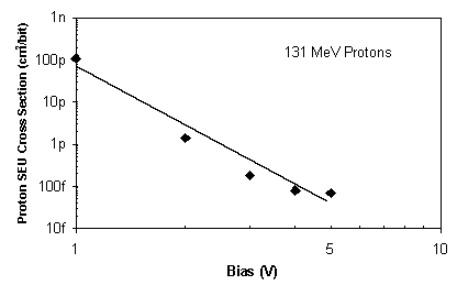
SRAM memory cells are of flip-flop design having two stable states. In
SRAMs SEU is influenced by the generated charge as well as by the shape
of the resulting current pulse [28]. Operating conditions can be very
critical. The high sensitivity of some SRAMs to the operating voltage
(Fig. 9) has led to the proposal to use groups of such SRAMs in
space as coarse multichannel devices detecting different threshold LETs
according to their operation voltage settings [29]. Such arrangement
would have the advantage that they would not suffer from the pulse
pileup problems that normal surface barrier detectors may encounter.
Fig. 8 (a) DRAM Single Event Upset cross section versus particle energy transfer [26]
(b) SEU cross section for different types of 16 MB-DRAMs versus proton energy [27]
Fig. 9 SEU cross section versus bias for 256 k SRAM exposed to protons, from [28]
4.2.3. Pacemakers
Pacemakers and defibrillators deserve special attention, because with
these one wants to make absolutely sure that no detrimental effects can
occur due to a malfunction of the electronics. There are two settings
to be investigated, the normal radiation background at ground level and
at airplane cruising elevations and the increased radiation levels
encountered during cancer therapy. In cancer therapy gamma rays or
electron radiation are predominantly used. Hence, one has to deal with
a total dose effect in this case. As miniaturization has progressed,
the safe limit of some devices has fallen to 2 Gy (1 Gy = 1 J/kg) which
is below the maximum therapeutic dose [30].
An extensive study of almost 600 implantable cardiac defibrillators in
which any SEU of the critical SRAMs due to cosmic rays was recorded and
corrected in a one-hour cycle revealed 22 upsets corresponding to a
failure rate per device of approximately 100 fit, i.e. to one failure
in 35 years [31] (fit stands for 'failure in time'; 1 fit corresponds
to one failure in 109 hours). One goal of this investigation was to
develop the tools to predict such low upset rates.
4.2.4. Power diodes and large-area detectors
When the high-speed train system was put into operation in Germany in
1991, it became obvious that diodes and gate-turn-off thyristors in the
inverter systems of the engines failed catastrophically due to
avalanche multiplication initiated by cosmic rays, i.e. by neutrons and
protons (compare Fig. 5b). The burnout currents in these systems
reached 100 kA. The cause was not immediately evident, because the
failures occurred at voltage levels of about half the rated voltage
[32]. At about the same time, similar failures were observed when
high-voltage detectors were tested in particle beams [33]. In the
meantime it has become clear that this type of failure limits the use
of high-voltage devices in many applications even at ground level. The
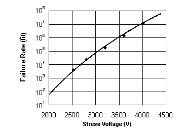
failure rate is extremely voltage dependent. In Fig.10 an example is
given for a diode with a rated voltage of 4500 V. Not every
multiplication event leads to destruction [34]. Non-destructive events
were measured in a fashion as indicated in Fig. 12 with charge
multiplication factors of 104. When burnout occurred it happened within
100 ns after the onset of multiplication [34]. Burnout cannot be
prevented in these large devices through external means, because the
internal capacitance stores sufficient energy for the destruction.
Fig. 10 Cosmic ray initiated failure rate of 4500 V power diode versus voltage [32]
4.2.5. Bipolar transistors and vertical MOSFETs
Bipolar transistors and power MOS field effect transistors are
seemingly quite different devices, because during normal operation
MOSFETs-transistors are unipolar. However, when it comes to SEUs these
devices exhibit similar behavior, because the failure of
MOS-transistors is often due to a parasitic transistor.
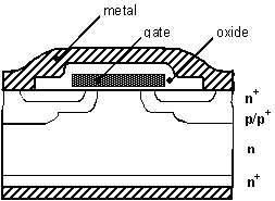
Fig. 11 depicts a crosscut through a power MOSFET. The parasitic
transistor is formed by the n+ - p – n – n+ layers. MOSFETs may also
fail due to gate rupture. This is more likely when the ion hits the
device in the gate area, whereas the transistor type failure may be
dominant when the device is hit in or outside of the the gate area. The
transistor-type failure is a typical second breakdown event, i.e. the
current generated by the absorbed ion is amplified by the transistor to
a level that the blocking voltage can no longer be sustained. Typical
for this type of failure is a breakdown delay of the order of a
microsecond. Burnout can be prevented during testing by external
current limiting or by a fast turn-off of the external circuit.
Fig. 11 Crosscut through power MOSFET
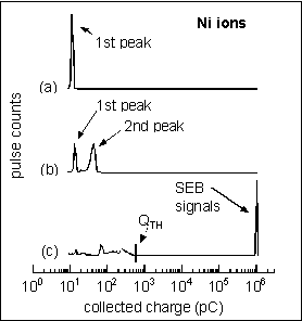
A typical behavior of a power MOSFET irradiated with nickel ions at
different voltage levels is shown in Fig. 12. The device is
operated like a detector [35]. At low voltage only the primary signal
is recorded. As the voltage is increased an amplified signal appears.
The first peak may shift due to some multiplication. If the voltage is
further increased, the amplified signal reaches a critical level Qth
where burnout occurs, resulting in a large SEB signal.
Fig. 12 Generated charge in a power MOSFET at increasing voltage levels [35]
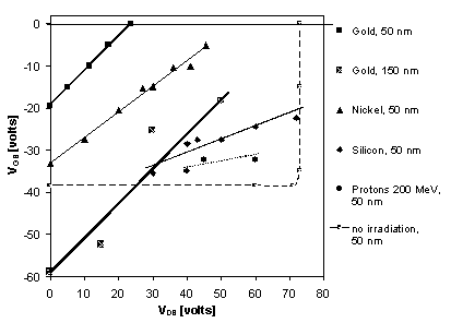
Gate rupture seems to be more of a problem for low-voltage MOSFETs. Fig
13 depicts a collection of data from [36]. The thickness of the n-type
epitaxial layer of these power MOSFETs was approximately 7 µm.
The minimum range of the ions used for the irradiations was 28
µm. In the case of the gold ions the ionization of the n-layer
was obviously so strong that the space charge layer could no longer be
supported (compare Fig. 4). The maximum voltage supported by the gate
oxide went down to about half its original value independent of the
oxide thickness. The influence of the protons is due to short-range
secondary nuclei, mostly lighter than silicon, generated in nuclear
reactions. Thus the results fit well into the general scheme.
Fig. 13 Gate rupture in 60 V- MOSFETs with 50 nm and 150 nm gate oxide thickness.
Variation of gate and drain voltage as well as of the ions used for irradiation. Selected from [36].
5. References
[1] J.F. Ziegler, J.P. Biersack, U. Littmark, "The Stopping and Range of Ions in Solids", Pergamon Press, 1985
[2] J.F. Ziegler , J.P. Biersack, "SRIM/TRIM, The
Stopping and Range of Ions in Matter/ The Transport of Ions in Matter",
http://www.srim.org, 1998
[3] B.C. MacEvoy, "Defect Evolution in Silicon
Detector Material", Nucl. Instr. Meth. Phys. Res., A 3888, 1997, 365-369
[4] B.J. Baliga, Power Semiconductor Devices, PWS Publishing Company, 1995
[5] J.R. Srour, D.H. Lo, "Universal Damage Factor
for Radiation-Induced Dark Current in Silicon Devices", IEEE Transact.
Nucl. Sci. 47, 2000, 2451-2459
[6] S.J. Watts, J. Matheson, I.H. Hopkins-Bond, A.
Holmes-Siedle, A. Mohammadzadeh, R. Pace, "A new model for
generation-recombination in silicon depletion regions after neutron
irradiation", Transact. Nucl. Sci. 43, 1996, 2587-2594
[7] W. Wondrak, "Erzeugung von Strahlenschäden
in Silizium durch hochenergetische Elektronen und Protonen",
Dissertation, Universität Frankfurt/M, 1985
[8] R.O. Carlson, Y.S. Sun, H.B. Assalit, "Lifetime
Control in Silicon Power Devices by Electron or Gamma Irradiation",
IEEE Transact. Electr. Dev. ED-24, 1977, 1103-1108
[9] H.H.K. Tang, "Nuclear physics of cosmic ray
interaction with semiconductor materials: Particle-induced soft errors
from a physicist's perspective",
IBM J. Res. Devel. 40, 1996, 91-108
[10] G.R. Srinivasan, H.K. Tang, P.C. Murley, "
Parameter-Free, Predictive Modeling of Single Event Upsets Due to
Protons, Neutrons, and Pions in Terrestrial Cosmic Rays", IEEE
Transact. Nucl. Sci. 41, 1994, 2063-2070
[11] C.M. Hsieh, P.C. Murley, R.R. O'Brien, "A
Field-funneling Effect on the Collection of Alpha-Particle-Generated
Carriers in Silcon Devices", IEEE Electr. Dev. Let. EDL-2, 1981, 103-105
[12] D. Binder, E.C. Smith, A. B. Holman, "Satellite
Anomalies from Galactic Cosmic Rays", IEEE Transact. Nucl. Sci. 22,
1975, 2675-2680
[13] T.C. May, M.H. Woods, "Alpha-Particle-Induced
Soft Errors in Dynamic Memories", Transact. Electr. Dev. ED-29, 1979,
2-9
[14] J.F. Ziegler, "Terrestrial cosmic rays", IBM J. Res. Devel. 40, 1996, 19-39
[15] J.C. Pickel, "Single-Event Effects Rate Prediction", IEEE Transact. Nucl Sci. 43, 1996, 483-495
[16] E.L. Petersen, "Approaches to Proton
Single-Event Rate Calculations", IEEE Transact. Nucl. Sci. 43, 1996,
496-504
[17] P.C. Murley, G.R. Srinivasan, "Soft-error Monte
Carlo modeling progam, SEMM", IBM J. Res. Devel. 40, 1996, 109-118
[18] "Particle Accelerators Around the World",
http://www-elsa.physik.uni-bonn.de/Informationen/accelerator_list.html
[19] P. Rai-Choudhury, J. Bartko, J.E. Johnson,
"Electron Irradiation Induced Recombination Centers in Silicon –
Minority Carrier Lifetime Control", IEEE Transact. Electr. Dev., ED-23,
1976, 814-818
[20] J. Vobecký, P. Hazdra, J. Homola,
"Optimization of Power Diode Characteristics by Means of Ion
Irradiation", IEEE Transact. Electr. Dev. 43, 1996, 2283-2289
[21] F.-J. Niedernostheide, H.-J. Schulze, U.
Kellner-Werdehausen, A. Frohnmeyer, G. Wachutka, "Radiation-Induced
Defects Utilized for Performance Tailoring in High-Power Devices",
DECON 2001, Electrochem. Soc. Proc. Vol. 2001-29, 2001, 112-120
[22] Records of NSREC are published in 'IEEE
Transactions on Nuclear Science', those of RADECS in the IEEE
Conference Records.
[23] Special issue "Terrestrial cosmic rays and soft errors", IBM Journ. Res. Devel. 40, 1996
[24] G. Lindström et al. , "Radiation Hard
Silicon Detectors - Developments by the RD48 (ROSE)
Collaboration", Intern. Symp. Dev. Appl. Semicond. Tracking
Detectors", Hiroshima, 2000, Nucl. Instr. & Meth. in Phys. Res. A
466, 2001, 308-326
[25] L.Z. Scheick, S.M. Guertin, G.M. Swift,
"Analysis of Radiation Effects on Individual DRAM Cells", IEEE
Transact. Nucl. Sci. 47, 2000, 2534-2545
[26] S. Duzellier, R. Ecoffet, "Recent Trends
in Single-Event Effect Ground Testing", Transact. Nucl. Sci. 43, 1996,
671-676
[27] J.F. Ziegler, M.E.Nelson, J.D. Shell, R.J.
Peterson, C.J. Gelderloos, H.P. Muhlfeld, C.J. Montrose, "Cosmic Ray
Soft Error Rates of 16-Mb Memory Chips", IEEE Journ. Solid-State Circ.
33, 1998, 246-252
[28] L.B. Freeman, "Critical charge calculations for
a bipolar SRAM array", IBM J. Res. Devel. 40, 1996,119-129
[29] P.J. McNulty, L.Z. Scheick, S. Yow, A.B.
Campbell, M.W. Savage, "Single-Chip Dosimeters to Accompany Photometric
Systems Flown in Space", IEEE Transact. Nucl. Sci., 48, 2001, 2039-2042
[30] J. Mouton, R. Trochet, J. Vicrey, M. Sauvage, B.
Chauvenet, A. Ostrovski, E. Leroy, R. Haug, B. Dodinot, F. Joffre,
"Electromagnetic and Radiation Environment Effects on Pacemakers"
RADECS 99, IEEE Conf. Rec. 2000, 34-38
[31] P.D. Bradley, E. Normand, "Single Event Upsets
in Implantable Cardioverter Defribrillators", IEEE Transact. Nucl. Sci.
45, 1998, 2929-2940
[32] H. Kabza, H.-J. Schulze, Y. Gerstenmaier, P.
Voss, J. Wilhelmi, W. Schmid, F. Pfirsch, K. Platzöder, "Cosmic
Radiation as a Cause for Power Device Failure and Possible
Countermeasures", IEEE Proc. 6th Internat. Symp. Power Semicond.
Devices & ICs, Davos, CH, 1994, 9-12
[33] G.Anzivino, J. Bai, B. Benscheikh, A. Contin, R.
DeSalvo, S. Fagen, H. He, L. Lui, M. Lundin, R.M. Madden, M.R.
Mondardini, M. Swazlowski, K. Wang, X. Xia, C. Yang, M. Zhao, "Failure
modes of large surface avalanche photo diodes in high-energy physics
environments", Nucl. Instr. Meth. Phys. Res.A 430, 1999, 100-109
[34] G. Soelkner, P. Voss, W. Kaindl, G. Wachutka,
H.K. Maier, H.-W. Becker, "Charge Carrier Avalanche Multiplication in
High-Voltage Diodes Triggered by Ionizing Radiation", IEEE Transact.
Nucl. Sci., 47, 2000, 2365-2372
[35] S. Kuboyama, S. Matsuda, T. Kano, T. Ishii,
"Mechanism for Single-Event Burnout of Power MOSFETS and Its
Characterization Technique", IEEE Transact. Nucl. Sc., 39, 1992,
1698-1703
[36] J.L. Titus, C.F.Wheatley, "Proton-Induced
Dielectric Breakdown of Power MOSFETs", Transact. Nucl. Sci. 45, 1998,
2891-2897